
Analyze with AI
Get AI-powered insights from this Mad Devs article:
This article continues the "Introduction to Prototyping with EasyEDA" series. In the first article, we talked about how to install EasyEDA and how to create a new project. If you missed Part 1, go check it out:

In part II, we will do the following: Walk through the process of creating circuitry for our device. Learn how to use the selector of components for devices. Master the main device design tools.
Ideation
If you clearly understand what your device is intended for, you will come up with a list of requirements and a step-by-step development plan. In any hardware project, you should start with the idea of the future device. You need to ask yourself a question: Which problem should this device solve?
To have an example, let’s imagine that we design a simple but useful device—a timer with adjustable delay. The implementation of such a device on discrete elements will enable us to cover the basic principles of circuit design, board simulation, and tracing.
Simple technical requirements for our device:
- Start by button.
- Triggering indication.
- Adjustable delay.
- USB(5v) power supply.
Action plan
Once we have decided on the task, it is necessary to list the main steps for its completion from a schematic perspective.
- Power supply. Search for a USB type connector.
- Main timer. Simple solutions o Основной таймер. Simple realization variants on discrete elements(without ICs).
- Selecting the pulse generator for indication.
- Output array of LEDs for indication. Calculation of consumption. The best way to control it.
Tooling
As we came up with the concept of our new device, let's analyze the basic tools for building its circuit.
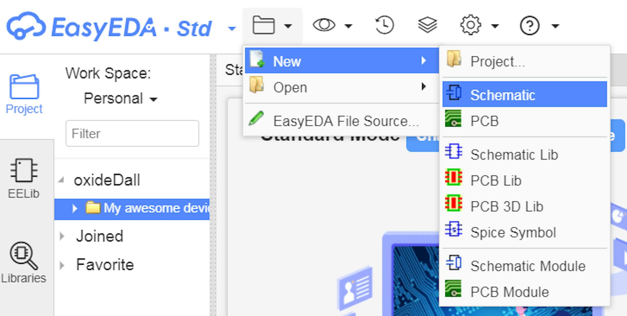
Let's go back to our project on EasyEDA and create a schematic file in the folder of our current project. To do this, we select it and click File > New > Schematic.
After that, you'll notice changes in your workspace. The toolbar, the properties panel, and the main working field of the document will be displayed.
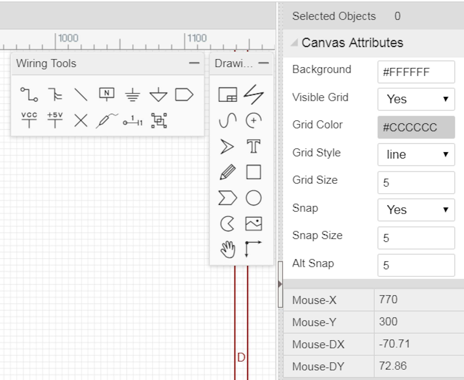
The Wiring Tools panel contains tools for connecting the elements by conductors and bus routing: data, ports, power; marking the voltage measurement point (necessary for simulation), renaming networks, and grouping the elements.
On the Drawing Tools panel, you can get access to a toolkit for creating and modifying graphic items: the document size editor (Document Settings), text editor (comments and simulation directives), a set of primitive graphic forms, drag-and-drop tool. There, you can also specify a document reference point.
To navigate in the workspace, use MMB to move and SCROLL to zoom.
Implementation
The schematic editor arranges the elements with a grid snap. With this EasyEDA tool, you can align the elements and create connections between them. Let's open and analyze the canvas parameters. To do it, click on the space on the canvas.
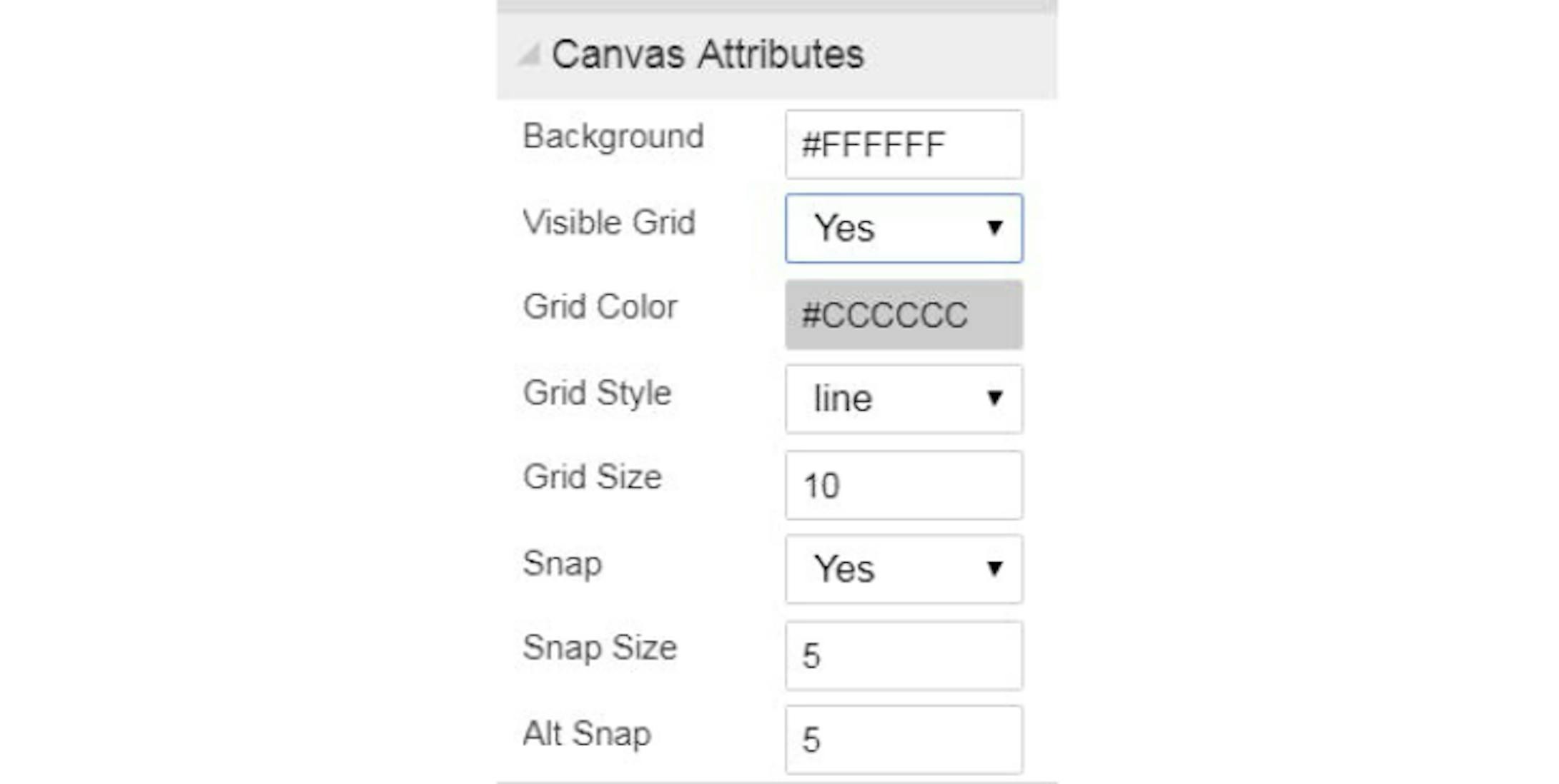
In the canvas settings, you can change the canvas color, enable or disable the grid, change the grid color, type, size, enable snapshots, and change the snap's basic and alternative sizes.
For quick placement of schematic components, EasyEDA has a library of common elements. Go to the EELib tab to expand the library.
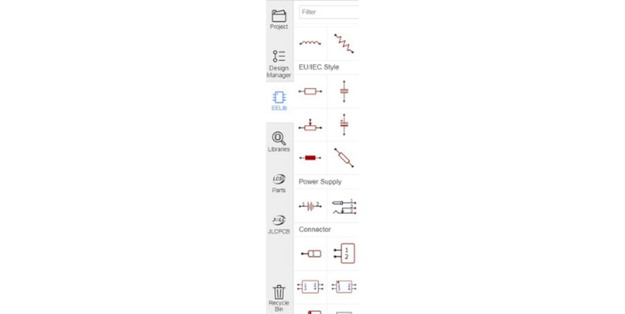
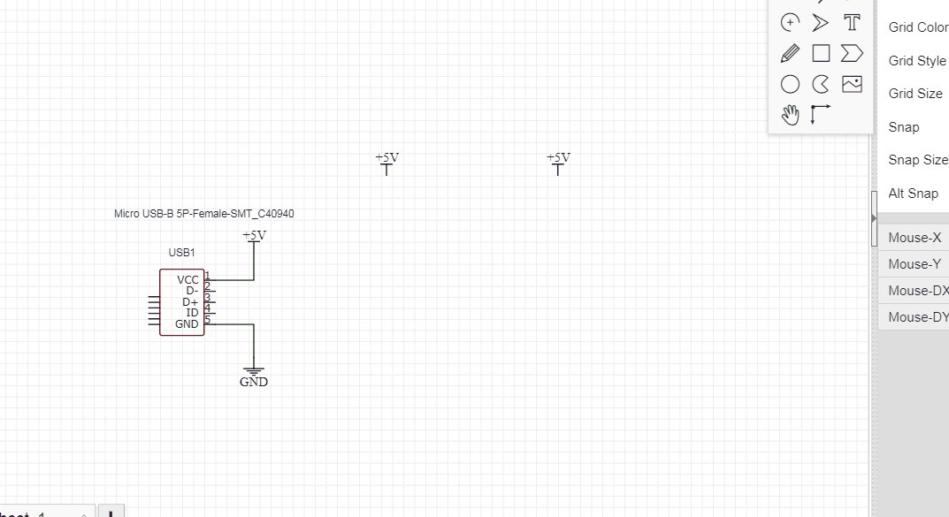
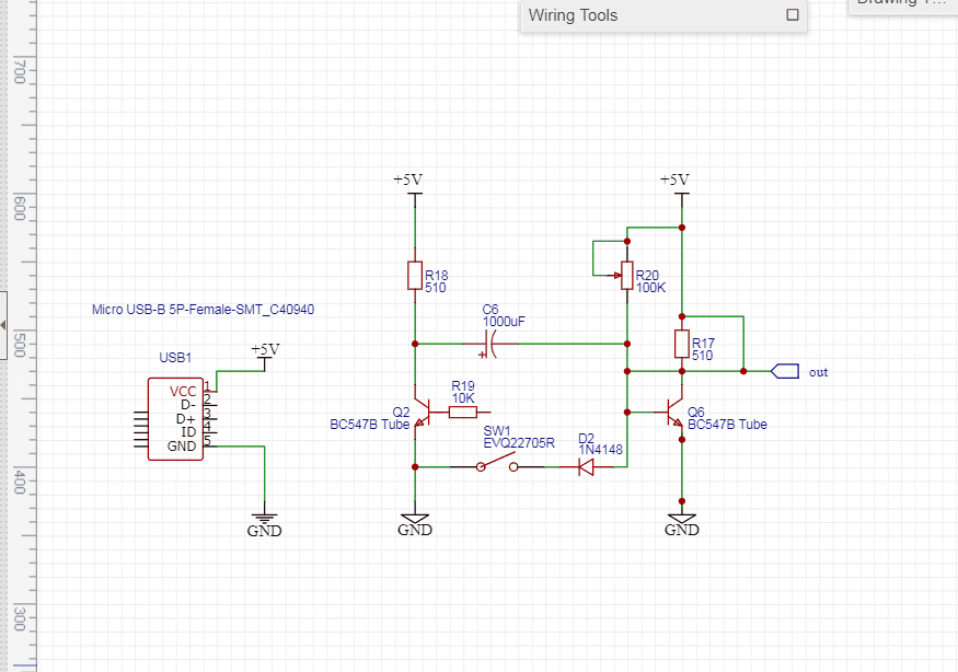
Following the design plan, we need to take care of the device's power supply first. Since we are going to power the device from the USB port, we will choose the corresponding element in the Connectors section.
We will use Micro USB for its ease of use and universal availability.
To open the list of items of one class, click on the arrow next to the item's image.
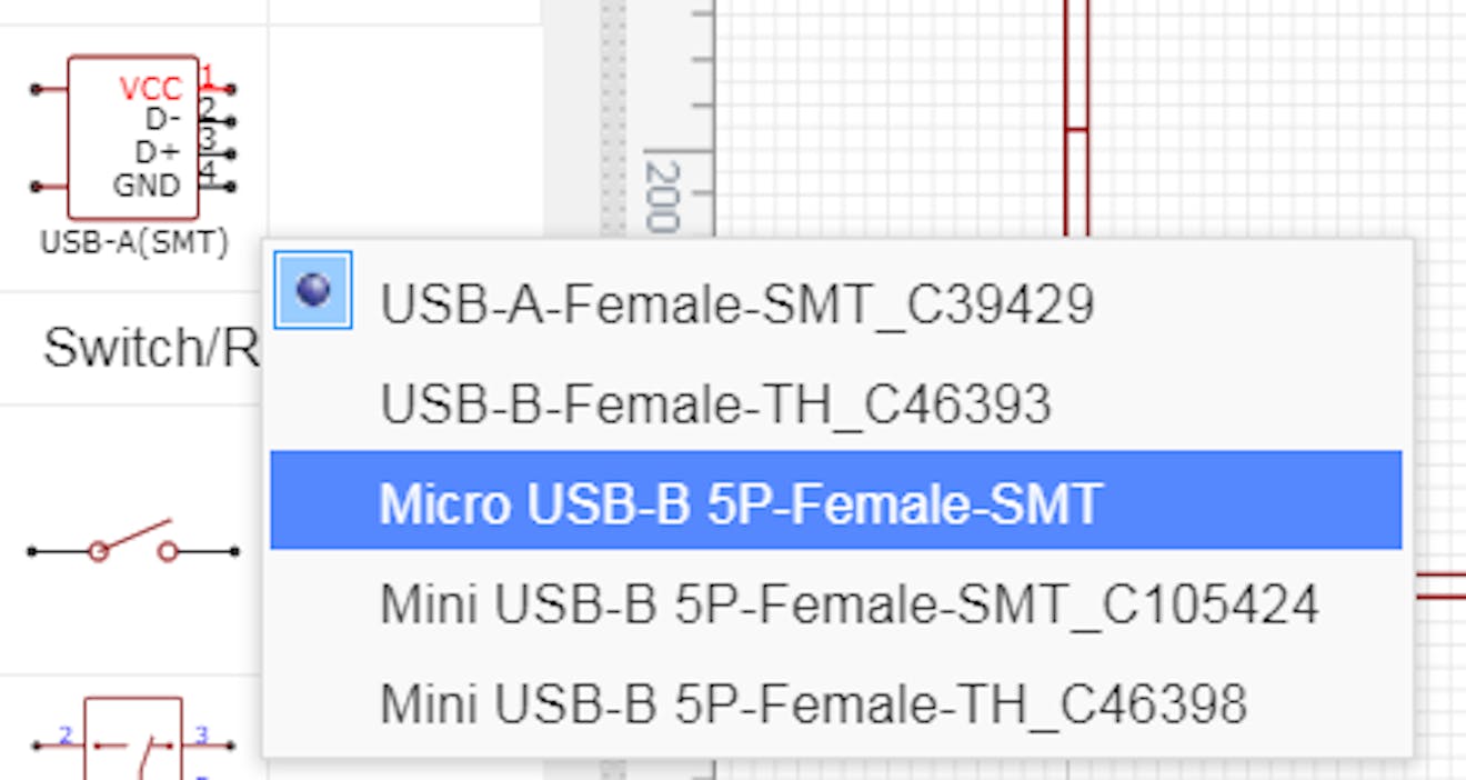
Then click on this item in EElib again, and after that, click on the document workspace. Use the Esc key to exit the item arrangement mode.
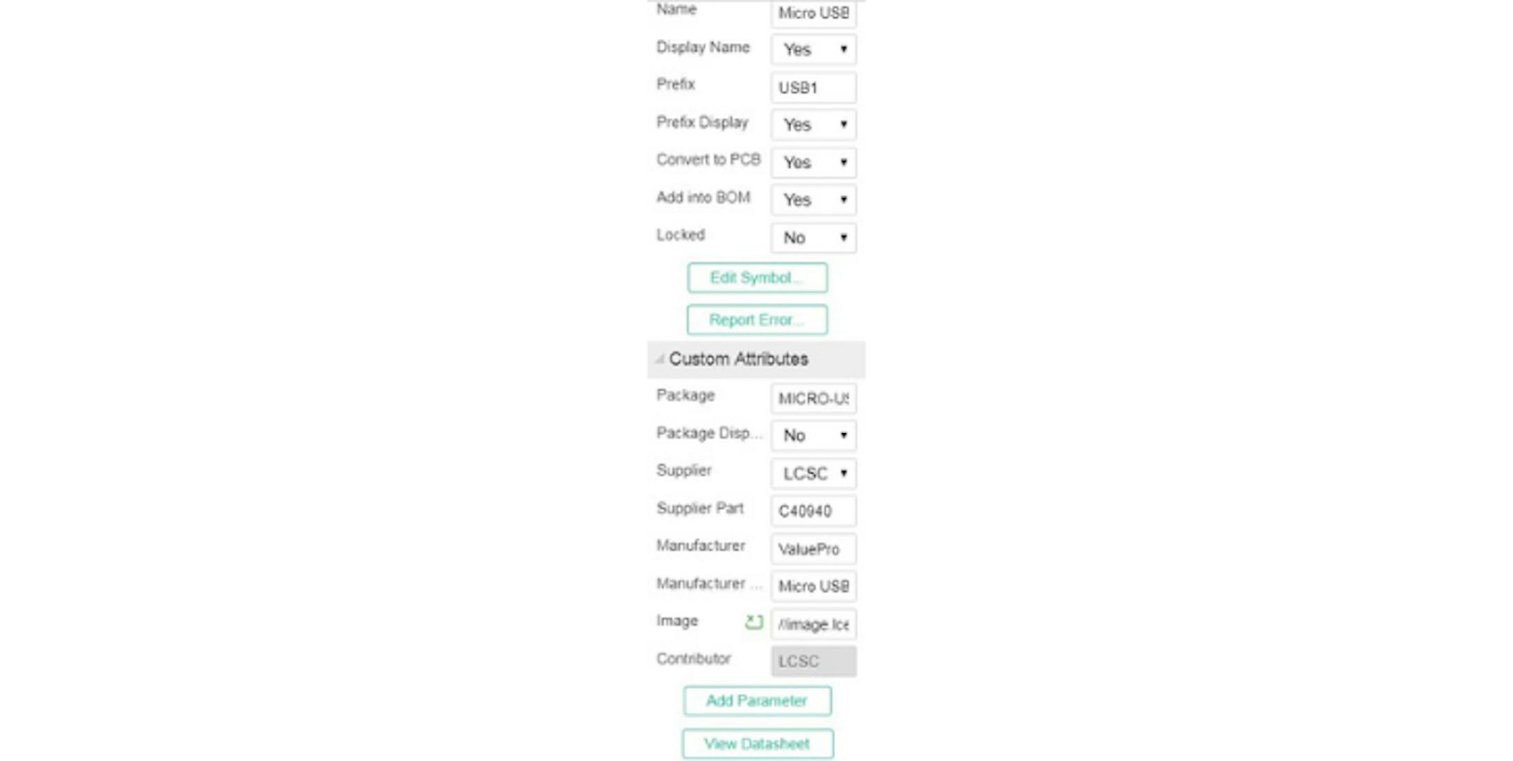
To view the properties of an element in the work field, select the corresponding option. There, you can set the location, view documentation, and information about the element supplier.
Installing ground and voltage buses in EasyEDA
To do this, select NetFlag +5v (USB uses 5V power) on the Wiring Tools panel and place it next to VCC at the USB input. After that, choose one of the designations of NetFlag GND (functionally, the designations of circuit lands do not differ; the division is caused by the differences in standards of individual countries). Then place the ground next to the GND output of the USB connector.
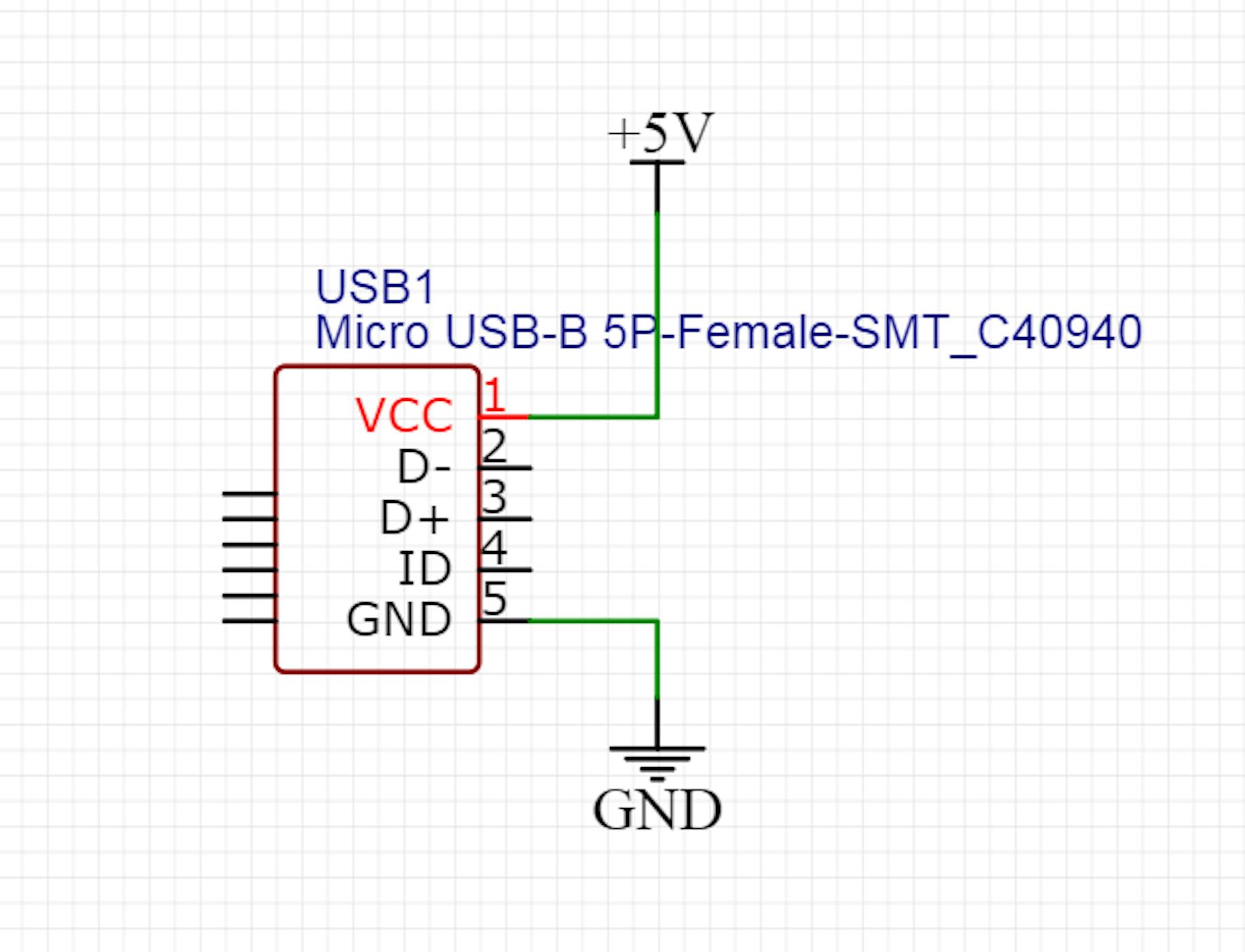
Use Wire (hotkey W) on the Wiring Tools tab to create connections between elements. With the wiring tool, point to the output pin of the VCC element, a dot will appear on it, click the dot to "take out" the wire. Connect it to the power bus, and also click on the point that appears.
Quick recommendations
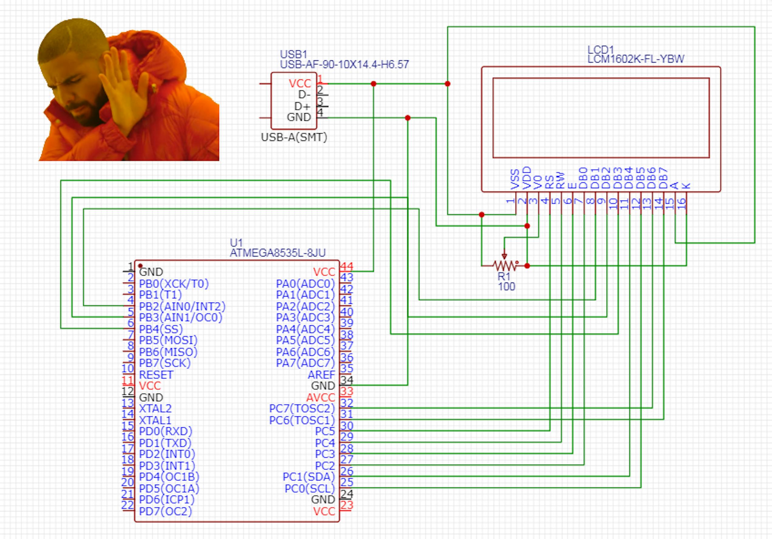
The power and data buses and the ports with similar names are connected. When we add the 5V bus again and connect it to some element, in the Simulation Mode and PCB Tracing mode, all the output ports of the elements where the 5V comes from will be connected to one point. Example of the schematic and the board:

The use of buses is convenient if the schematic has a large number of connections (many elements or data buses). However, you should not focus on only buses and ports. You should not focus on the use of only connections, either. The schematic is easy to read when wiring connections to key pins and using buses to multiple data ports. Examples of difficult- and easy-to-read schematics:
The data and power buses are wired, the wires intersect at many points, and it is easy to get tangled up in the connections and make an imperceptible error.
Most connections are made through ports. It is visually difficult to find all connection points of the same ports; you have to double-check them several times. On large schemes, finding all similar ports takes a lot of time.
Wires and elements rarely overlap, and it is easy to trace connections. With this circuit design, errors are hard to make and easy to find.
Even with a large number of connections and crossings, it is quite easy to trace the work of the circuit. Using bus bars in this example helps get rid of the heap of power connections. This makes it easier to understand the circuitry of the device.
Getting back to circuit design
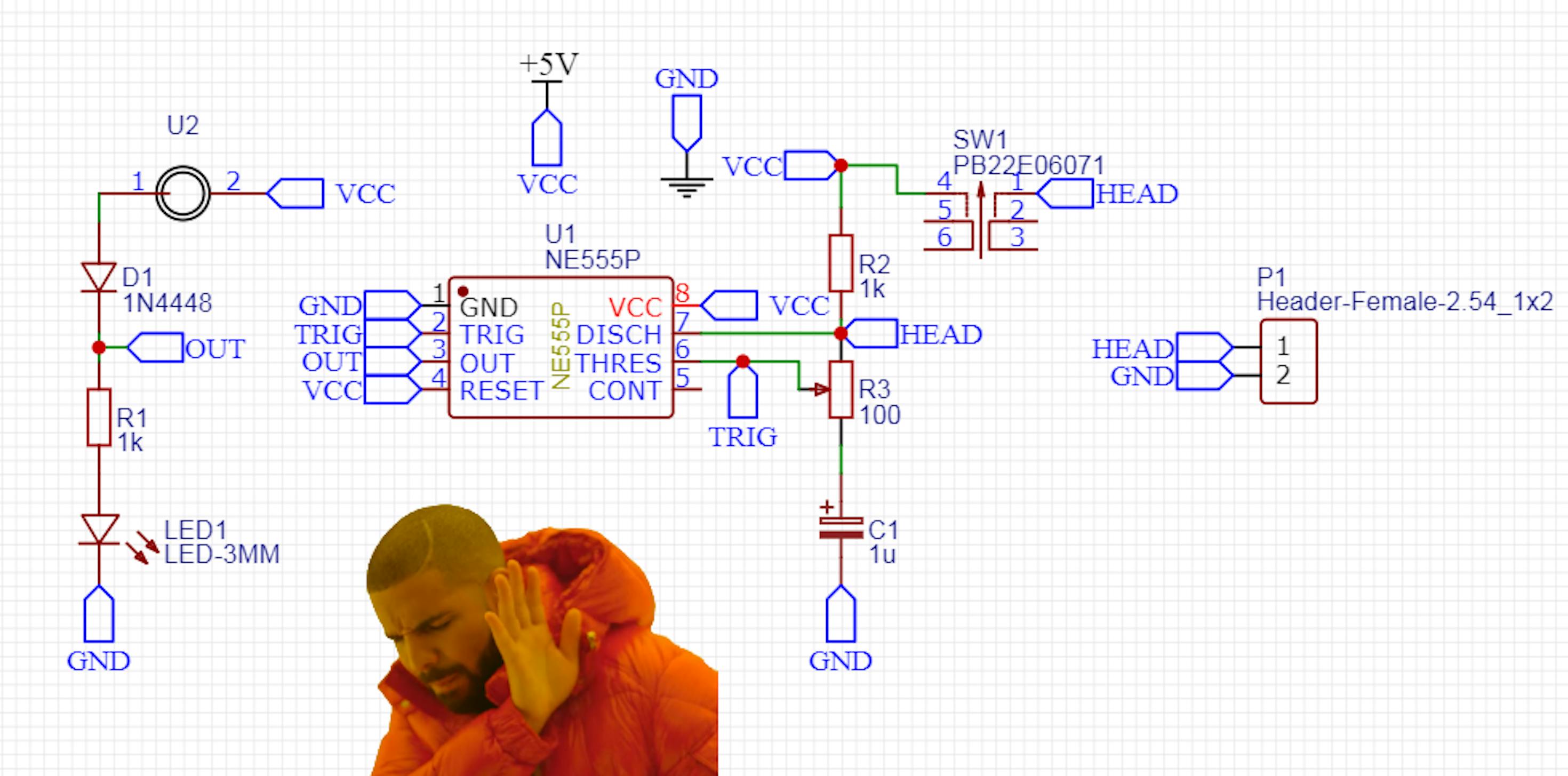
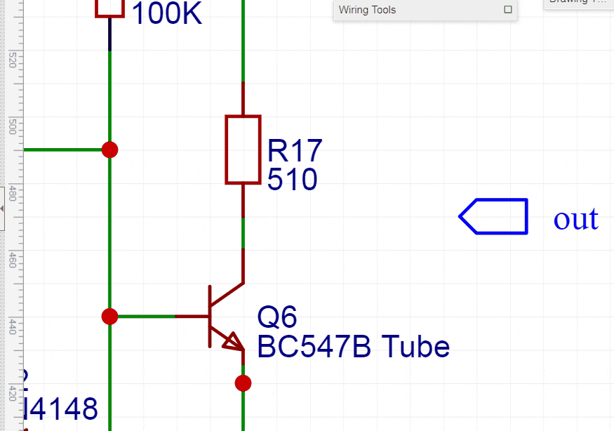
After the power supply has been connected, we can start designing the heart of our timer — monostable multivibrator. To provide an example of work with both discrete elements and chips in our schematic, we will use 2 timers, one on discrete elements, and the second using the known NE555 chip. The last one is necessary for setting the indication time.
Let’s start designing the first-timer. You can assemble it using the following diagram:
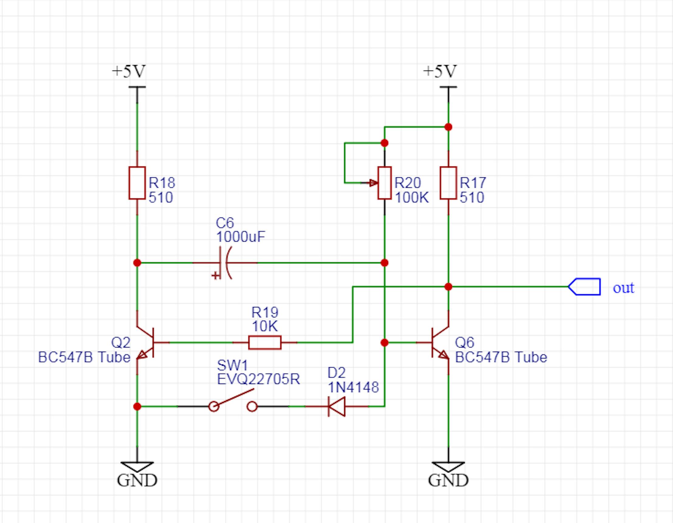
The function of this circuit is as follows: when SW1 is closed, a voltage pulse will be generated on the output pin. You can calculate the duration of the pulse using this equation:

where R20 stands for resistance in Ohms and С6 for capacitance in Farads.
In a nutshell, by changing the resistance R20, you can change the duration of the output pulse. The principle of operation and detailed description of transients in the scheme would make a good topic for a separate article, so we will just focus on the usage of this scheme in our project. To better understand how this timer works, you can browse websites specializing in electronics. The timer reacts to the fall of the pulse, it means that it will start working when the button is pressed, not released. We will consider the calculation of circuitry in more detail in one of the following articles.
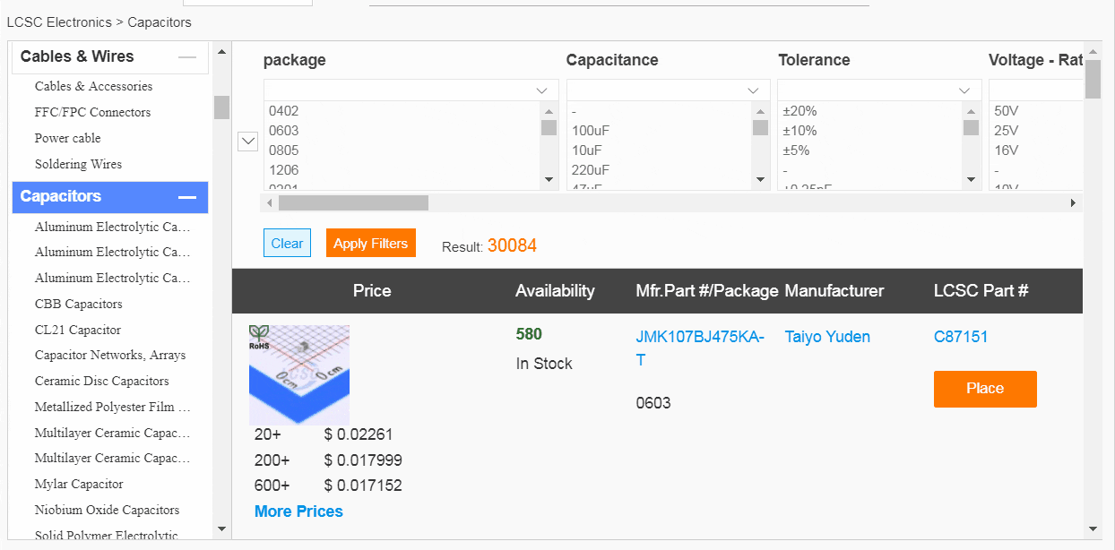
To ensure that our schematic has adequate information about the parts that can then be ordered later, it's better to use an LCSC parts selector.
To select the parts on the LCSC, click on the tab Libraries.
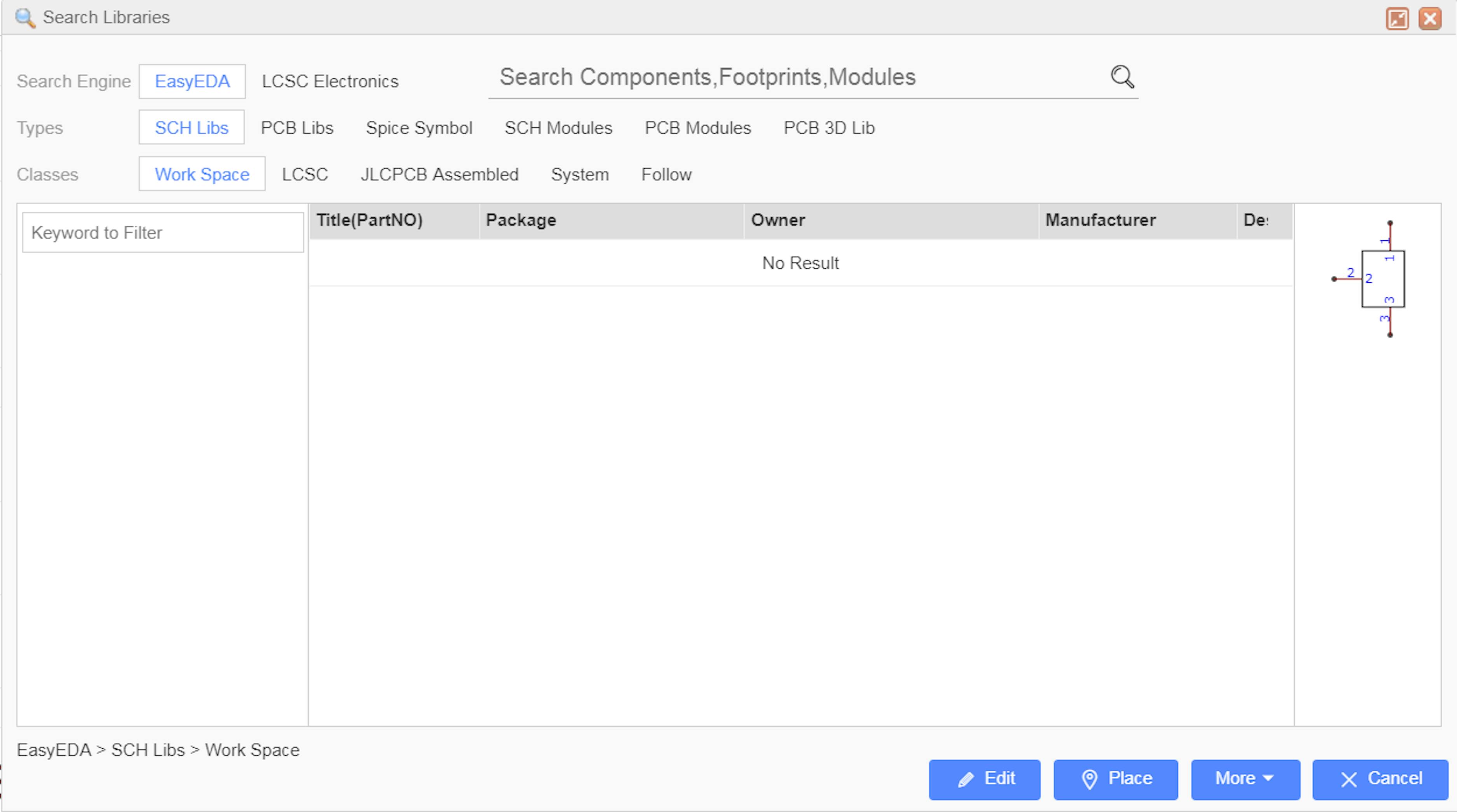
In the component search window, we have the option of enabling us to select a search engine. If you select EasyEDA, the search types from EasyEDA will appear:
- Types:
SCH Libs — the libraries of schematic elements.
PCB Libs — the libraries of circuit board components.
Spice Symbol — the libraries of simulation components.
SCH Modules — schematic modules (devices, sequences of devices).
PCB Modules — routing modules for including into circuit board.
PCB 3D Lib — 3D models of components for creating PCB 3d model.
- Classes:
Work Space — components of your work space and your team's workspaces.
LCSC — components from the LSCS market.
JLCPCB Assembled — components which can be assembled to the PCB after the manufacturing process is over (see the SMT icon).
System — components imported with a project from another IDE (i.e., KiCad, Eagle, etc.)
Follow — the components of users to whose updates you have subscribed.
After you have found and selected a component, press the Place button to place it on the workspace.
Select LCSC Electronics to open the web view of the LCSC website in the search box. Let's find several items using this search engine.
In our circuit, we have several resistors, a pair of BC547 transistors, a button, a capacitor, and a diode.
Let's start with the resistors:
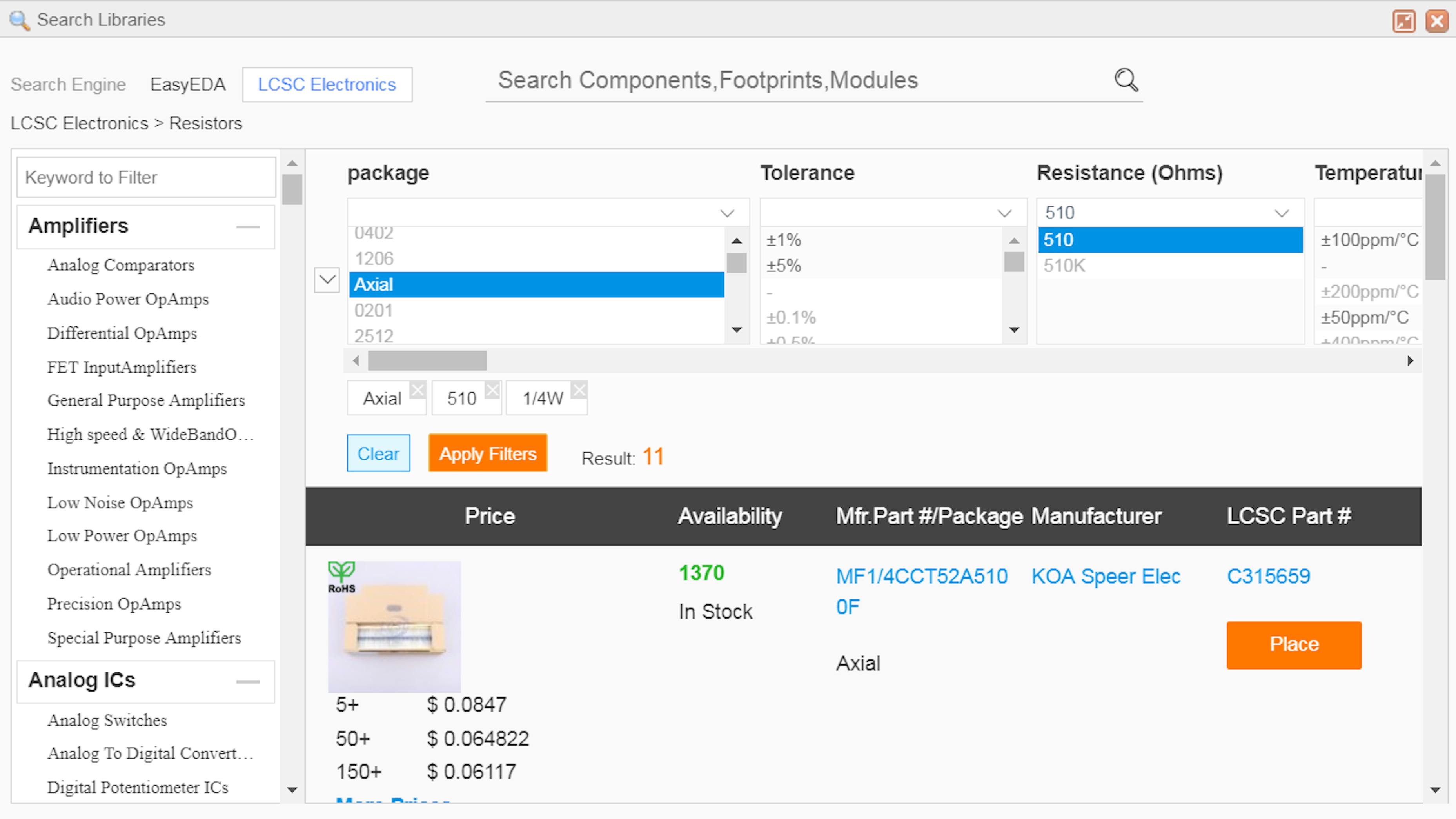
In the left column, select Resistors. There are many kinds of resistors with different parameters, materials, and production technologies available there.
We're interested in the resistors with the following parameters:
Package: Axial — package for placement through the holes in the board.
Resistance: 510 Оhm.
Power (Watts): Our timer works with low currents and low voltages, so the 0.25-watt power package is acceptable. The acceptable power can be calculated by the following formula:

Where is U voltage on the resistor, in our case 5V, R is the resistance. P is the resulting power consumption of a resistor. By calculation, power is equal to 0.04 Watts.
After selecting the search filters, you should select the manufacturer and then press Place to place the item on the schematic.
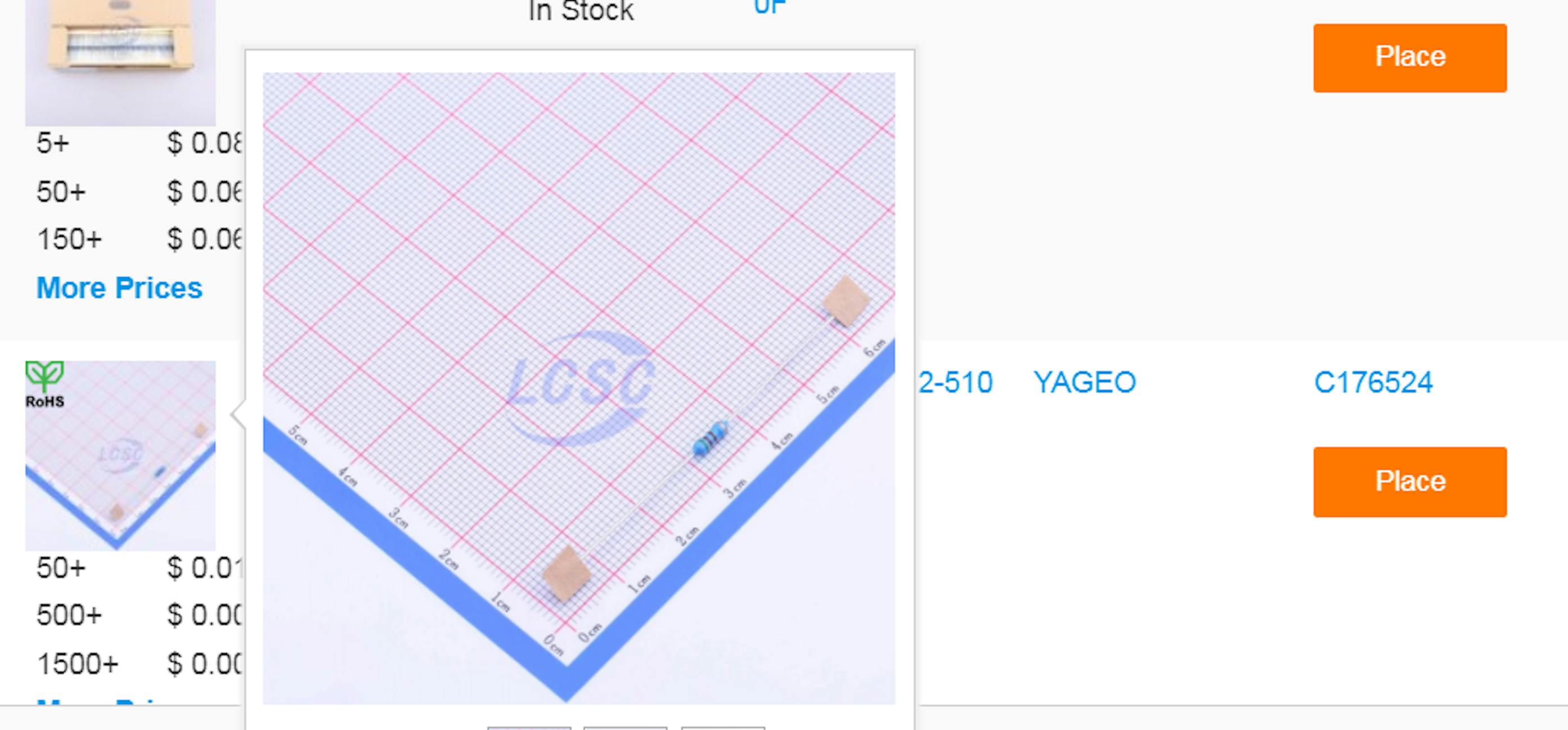
If you hover the mouse over the preview, the photo will be displayed in higher resolution.
To rotate the part, you can use the upper Rotate and Flip toolbar, or the Space hot key, or you can use Ctrl-C + Ctrl-V to copy and paste the part.
Use the following guidelines to find and place the remaining 10 KOhm resistors,100 KOhm potentiometer,1000 µF electrolytic capacitor, and BC547 transistors. Use the following filters to find them:
Potentiometer:
- Section: Resistors — Precision Potentiometer. Find with one rotation adjustment.
- Resistance: 100 KOhm — 300 KOhm. Choose any within this range.
- Package: Through Hole.
Capacitor:
- Section: Capacitors — Aluminium Electrolytic Capacitors — Leaded.
- Capacitance: 1000uF
- Voltage: 6.3V. USB is using a 5V supply. For our power supply, 6.3V is the closest voltage. You can pick the capacitor with a higher (not lower!) voltage.
I have chosen this capacitor. Please note that electrolytic capacitors are asymmetric — they have + and -.
Transistor:
BC547 is one of the most common transistors. It's analogous to the legendary Soviet Union transistor KT315. There's nothing special about it; the model defines all the characteristics. Small deviations depend on the manufacturer and batch, but for our project, they are not so important. I have chosen this transistor. To mirror the transistor vertically, use the Rotate and Flip menu.
Button, diode: I took them both from the standard EELib. All EELib components are linked to LCSC, so you can safely use them.
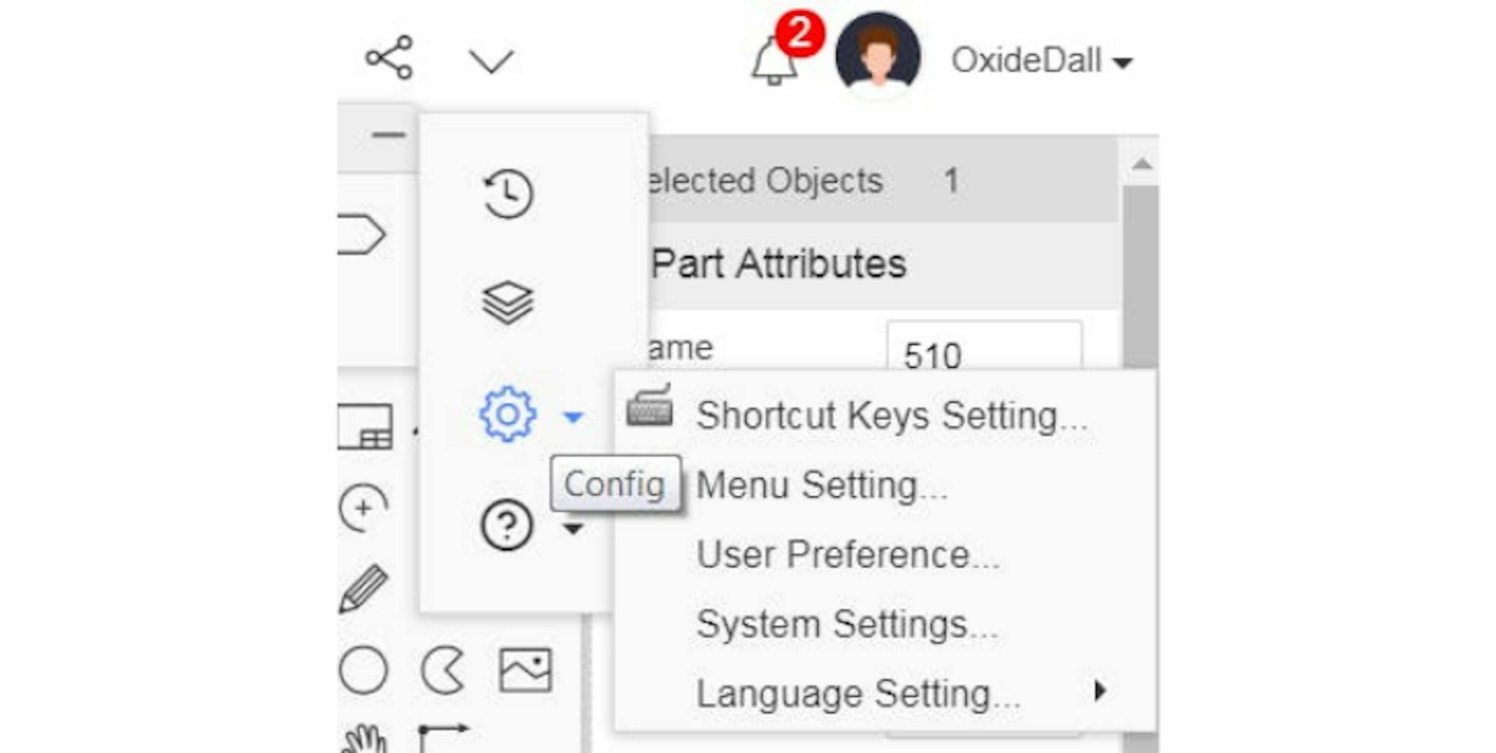
To make the design process more convenient, you can use the hotkeys. The list of all hotkeys with possibility of editing is in the Config — Shortcut Keys Settings menu:
The first-timer ensures the main delay is ready, now you need to design a timer setting the indication time. You can surely take the existing one, copy it, and connect its input to the output of the first-timer. To make a comparison with similar solutions and get familiar with the new type of elements, let's design the second time using one of the most popular chips, NE555.
This chip stands out from others as it can be applied everywhere (from LED flashing to rocket control), is cheap, and has table operation.
More detailed information about NE555 can be found in numerous sources on the Internet.
We're going to use the chip as a simple monostable multivibrator. The scheme is displayed below:
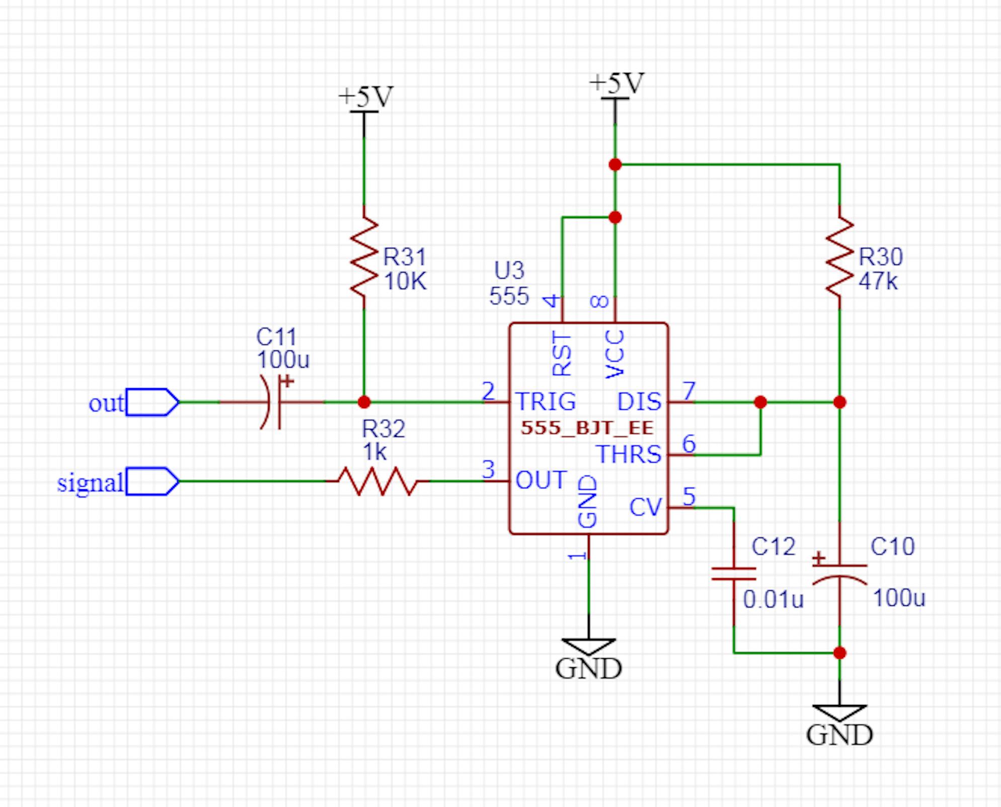
The function of the circuit is as follows: when a falling edge of voltage appears on the outpin, the chip fires a voltage pulse (VCC — 1.5V) at the chip output (pin 3). You can use this formula to calculate the duration of a pulse:

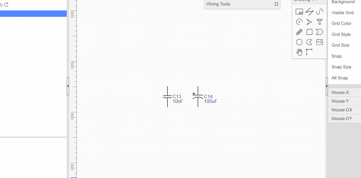
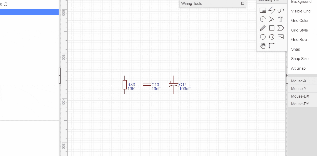
This schematic uses elements similar to the ones employed by the previous version of the timer, except for the non-polar capacitor and the chip itself.
We have already created a one-timer using elements soldered through holes in the board, so let’s create a second timer using surface mounting devices.
Surface mounting devices such as capacitors, resistors, diodes, and chips are manufactured according to standard sizes. The standard sizes for resistors in mm are as follows:
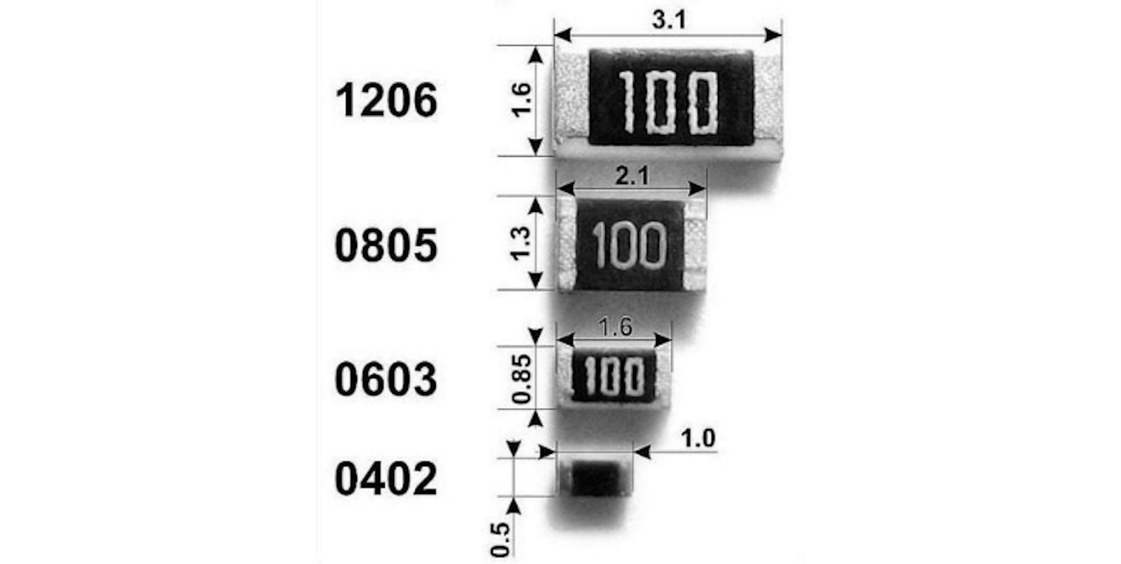
For the first experience with SMD, we will try to use the standard 1206. To take 1206 resistors and capacitors, select the corresponding filter in the search box. A tantalum capacitor can be used instead of an electrolytic capacitor:

Here’s the example illustrating a non-polar capacitor selection:
Here's the example illustrating a SMD resistor selection:
Here’s the example illustrating the selection of NE555 in SOP-8 package:
Now let's follow a further recommendation to finish the second part of our device.
Output stage
After the second timer has been designed, you need to add an indication unit to your device. I decided to add 9 red 5mm LEDs (consumption 20mA), you can choose other colors, LEDs are in the Optocouples & LEDs & Infrared — Light Emitting Diodes section.
The NE555 chip supports a maximum output current of 225mA. This is enough for 9 LEDs, but it is better to provide a margin. We will use the famous Darlington transistor, TIP122, for power amplification.
We will limit the LED current with SMD resistors. The following formula can be used to calculate the resistance to the LEDs:

where is U(r)— voltage on resistor.
U(led) — forward led voltage. You can take it from the datasheet (in my case, it's 2.4V)
I(led) — forward led current (in my case, it's 20mA).
Thus, for 5mm red LEDs, the resistance will be 130 Ohms.
The scheme is as follows:
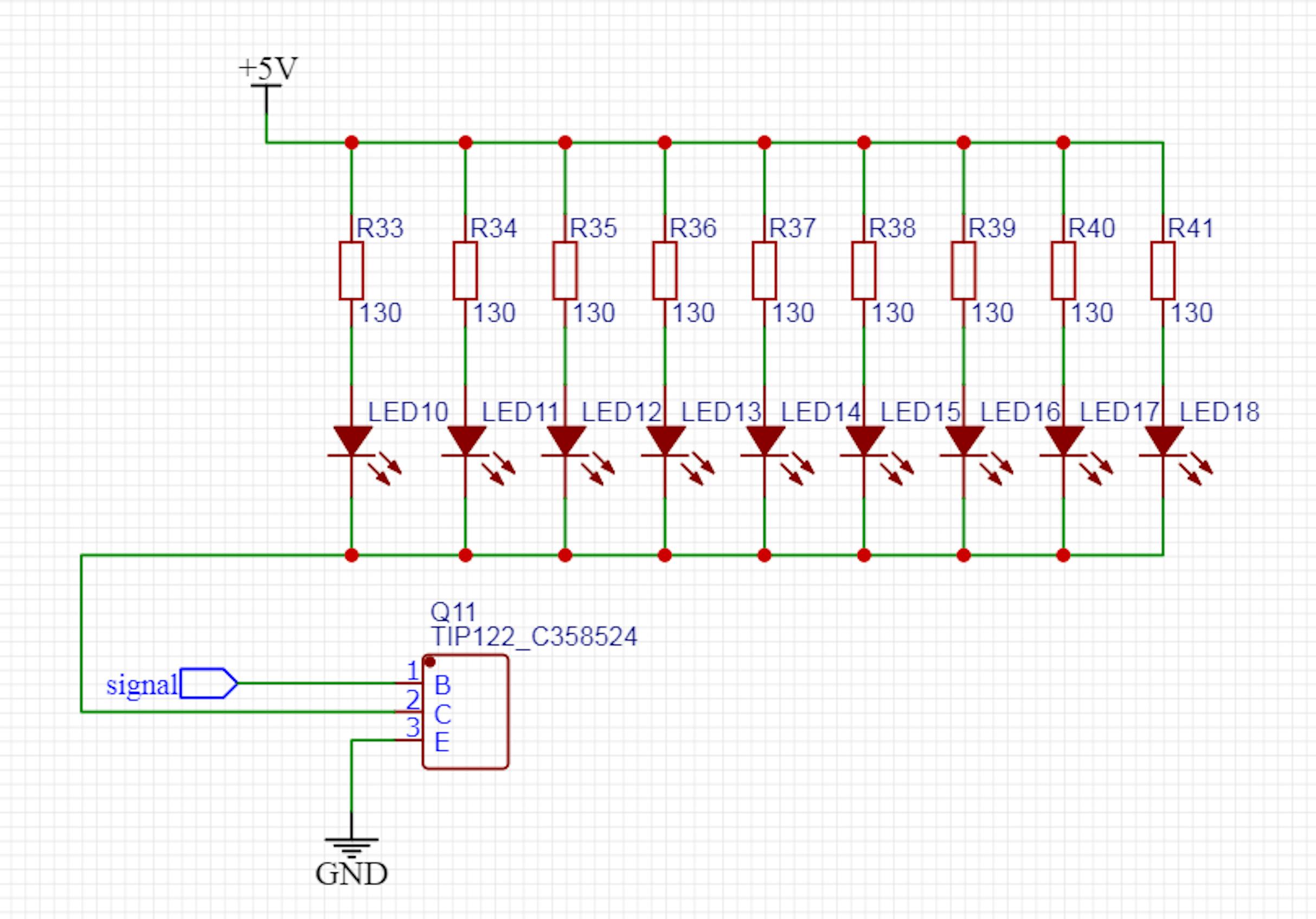
How does it work?
When current is applied from the NE555 to the TIP122 transistor base, it is opened to saturation, and the circuit C — E (collector—emitter) is opened, the LEDs are lit, everything is quite simple.
On completion of the wiring stage of the LED array, the circuitry of our device is finished. You only need to perform a simulation, which will result in minor corrections to the schematics.
Checking the connections
After you finish the circuitry, it needs to be checked. To do this, open the Nets folder on the Design Manager tab. In case some pins of components in your schematic are not connected to anything, or different buses are shorted (5V and ground for example), you will see a number of warnings.
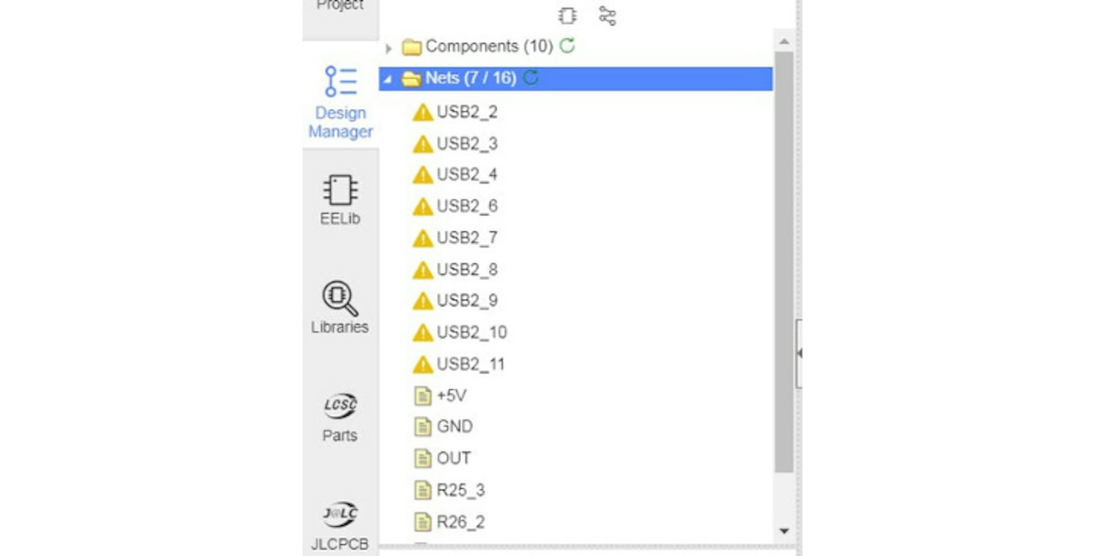
In this case, we have not connected the grounding contacts of the USB port. Let's fix this by connecting all the remaining USB port pins to the ground. It is better to leave the data pin unconnected, as it can be used to transfer information about the consumer to a voltage source.

Common mistakes
The following errors may occur during the schematic design:
- Overlapping the new track contact area of the element.
- Overlay of contact pads of elements. They seem to be connected, but in fact, they're not. There's no need to trivialize the size of the circuit. Minimizing the board saves cost, size of the device, and minimizing the circuit will add errors and minimize readability.
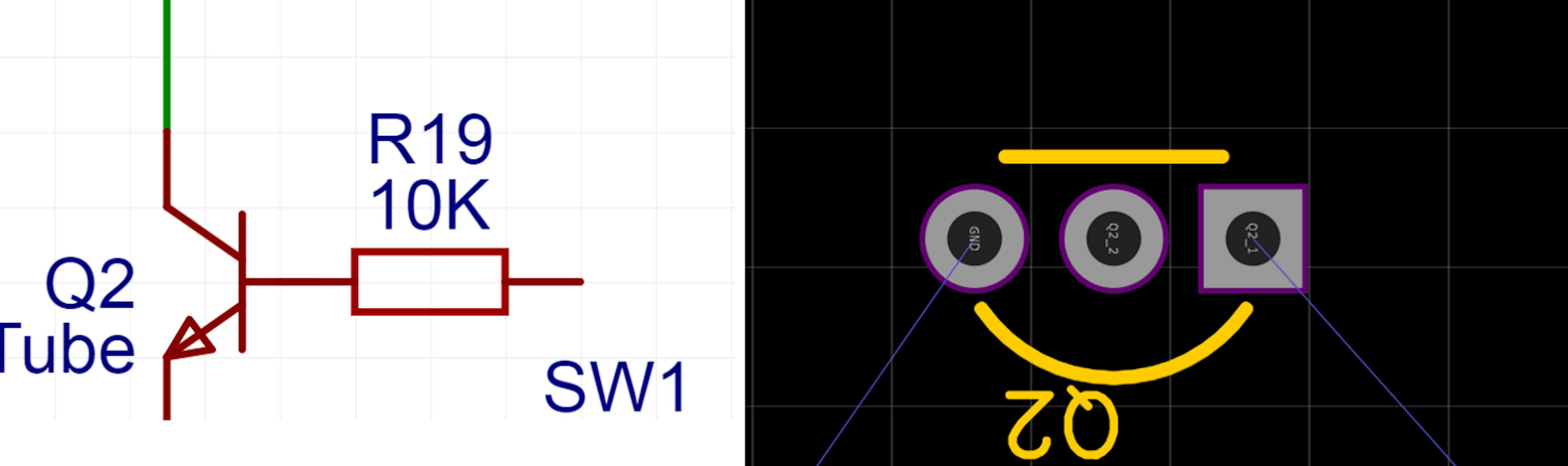
- The tracks are perpendicular to the contacts. When you move an item, you can shorten the tracks without noticing.
You can always check track connections to the contacts of the items on the Design Manager tab.
Conclusion
After reading this article hope you've gained knowledge and experience of using the EasyEDA service. With this knowledge, you can design the schematic of your device according to all the development rules.
In the next article, you'll get familiar with the tools for simulating the schematic of your device.


Latest articles here